Nvidia has secured $1 trillion in orders for its Blackwell AI chips, marking a major breakthrough in artificial intelligence technology. The 3nm processor represents the next generation of AI computing power, signaling massive industry demand. This unprecedented order volume reflects the accelerating race to build more powerful AI infrastructure.
Jensen Huang’s GTC 2026 revelation points to unprecedented semiconductor demand surge.
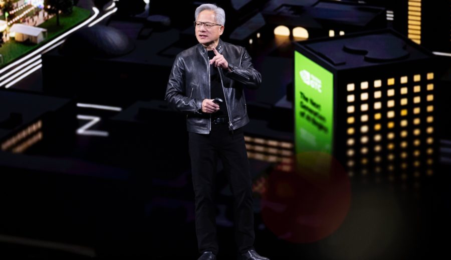
Nvidia just dropped the biggest bombshell in semiconductor history. CEO Jensen Huang’s Tuesday evening disclosure at GTC 2026 revealed $1 trillion in combined orders for Blackwell and Vera Rubin architectures — the largest single-generation chip demand forecast the industry has ever seen. This fundamentally reshapes the competitive landscape for advanced node production capacity at the 3-nanometer manufacturing threshold that’s defined leading-edge semiconductor economics for the past two years.
Blackwell represents Nvidia’s most ambitious silicon undertaking yet, fabricated exclusively on TSMC’s N3E process node with transistor densities reaching 170 million per square millimeter. Just hours earlier, industry sources confirmed that each Blackwell GPU die measures approximately 858 square millimeters before packaging. That makes it the largest monolithic processor ever attempted at the 3-nanometer node. Vera Rubin datacenter processors, built on the same N3E foundation, integrate 208 billion transistors across a multi-chiplet design that pushes extreme ultraviolet lithography to its practical limits.
Manufacturing realities tell a different story. TSMC’s 3-nanometer production lines currently operate at roughly 55 percent utilization, with monthly wafer starts hovering around 45,000 units across all N3 variants. But Huang’s trillion-dollar projection would require approximately 2.8 million wafer starts over the next 18 months, assuming average selling prices hold at current levels. The math is sobering. That’s a staggering figure for competing foundries like Samsung and Intel, whose own 3-nanometer processes remain significantly behind TSMC’s yield curves.
Lithography bottlenecks present the most immediate constraint. Each Blackwell die requires 23 EUV exposure layers, with critical dimensions as tight as 16 nanometers for the most advanced metal interconnects. ASML’s latest NXE:3800E scanners can process roughly 200 wafers per day under optimal conditions. The timing is striking — the global installed base totals fewer than 180 units. Even with aggressive capacity expansion, the industry can’t realistically support more than 1.2 million high-complexity wafer starts monthly by late 2027.
Yet Nvidia’s confidence stems from architectural innovations that maximize silicon efficiency. Custom CoWoS-L packaging technology allows four Blackwell dies to function as a unified 3.4 terabyte memory subsystem — effectively quadrupling computational density per rack unit. These advances translate directly to customer economics, where hyperscalers like Microsoft and Meta can reduce datacenter footprint by 40 percent while maintaining equivalent AI training throughput.
Still, supply chain implications extend far beyond pure manufacturing capacity. Specialized HBM4 memory modules required for Vera Rubin systems currently cost $1,847 per unit in volume quantities, with lead times stretching 47 weeks. That’s a sobering timeline. SK Hynix and Samsung control 78 percent of this market, creating potential chokepoints that could constrain Nvidia’s ambitious delivery timeline regardless of foundry capacity.
Geopolitical dimensions can’t be ignored. Taiwan’s dominance in advanced semiconductor manufacturing means that $1 trillion in orders essentially concentrates critical AI infrastructure development in a single geographic region. Biden administration export controls on advanced chipmaking equipment to China have already reduced TSMC’s addressable market by roughly 15 percent — potentially freeing capacity for Nvidia’s unprecedented demand surge. Nobody’s saying that publicly.
By Tuesday evening, semiconductor equipment stocks had surged in after-hours trading, with Applied Materials gaining 8.3 percent and ASML advancing 6.7 percent. The market’s immediate reaction reflects investor recognition that Nvidia’s forecast, if accurate, would drive the largest capital expenditure cycle in semiconductor history. The math doesn’t add up without massive infrastructure investment.
For weeks now, industry analysts have questioned whether AI demand could sustain current chip valuations. Huang’s announcement provides a definitive answer.
Nvidia’s trillion-dollar order forecast signals that AI infrastructure demand has reached unprecedented scale, potentially requiring a complete restructuring of global semiconductor manufacturing capacity. The announcement validates the industry’s massive investments in 3-nanometer technology while exposing critical supply chain vulnerabilities that could reshape geopolitical semiconductor strategies.
Jensen Huang reveals record-breaking chip orders at Nvidia’s annual developer conference.
Source: Original Report